An open disaggregated programmable infrastructure vision
Taking the new technical possibilities that appeared in the last years, I developed more and more my personal vision on the perfect open disaggregated programmable Telco CO/SP and Data Center infrastructure architecture. This post is a first in a series describing this personal vision.


During the long years consulting and working on large (and small) Telco/Service Provider networks, Data Center infrastructures and Enterprise ICT environments I've seen lots of different customer requirements lists, architectures and corresponding designs and implementations. Learning from the good and the bad (and the ugly) and using the new technical possibilities that appeared in the last 2 years, I developed more and more a vision on the perfect programmable Telco Central Office (CO)/Service Provider (SP) and (hyper scale) Data Center (DC) architecture. This blog post is the first in a series and is a high level write down of this vision and ideas, more specific details about specific parts (especially about the Fabric/Networking and Control part) will follow in later posts.
Probably parts of this vision and ideas are for some of you already a (nearby) reality (or a no-brainer!), but during the last months I've learned there are lots of people not aware of new technologies that can help with networking, compute and storage implementation problems. Hopefully this write down will also help people with that.
Vision
What I want to create is a flexible and high performant programmable compute, memory, storage and networking infrastructure architecture (and design) that is usable in small locations (server rooms of Enterprise offices), medium locations (small to medium central offices) or large locations (large private Telco/SP/Enterprise DC or public DC provider) and can be easily be scaled up and down and changed for functional use and financial stability.
The most important thing I've learned over the years that there is not much difference in a public/enterprise DC and a Telco/SP location, the only thing different is the difference in numbers of the used integrated components. In Telco CO/SP racks there is more emphasis on the networking components and less on compute and storage, with DC racks its the other way around but generically the same hardware components are used!
By generalizing those hardware components by disaggregating them somewhat more, it should be possible to define an architecture and create a design where by mixing and matching of generic hardware modules (and by using generic control software) you can create a specific implementation instance of a Infrastructure Point of Delivery. If multiple vendors of hardware would also going to support those (new or existing) public, standards based modules then mixing modules from several vendors in one Point of Delivery would become a real possibility...
Infrastructure Point of Delivery
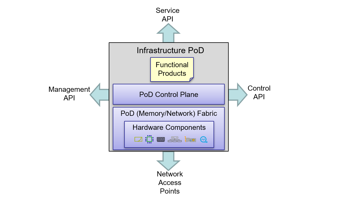
My definition of a Infrastructure Point of Delivery (PoD) is:
"A installation of network, compute, memory, storage, control and application components that work together to deliver infrastructure services. The PoD is a repeatable design pattern, and its modules maximize the modularity, scalability, and manageability of networks & data centers."
The PoD should be build from open, standardized, interoperable hardware modules based on open technologies and be composable by open, standardized, interoperable (control plane) software!
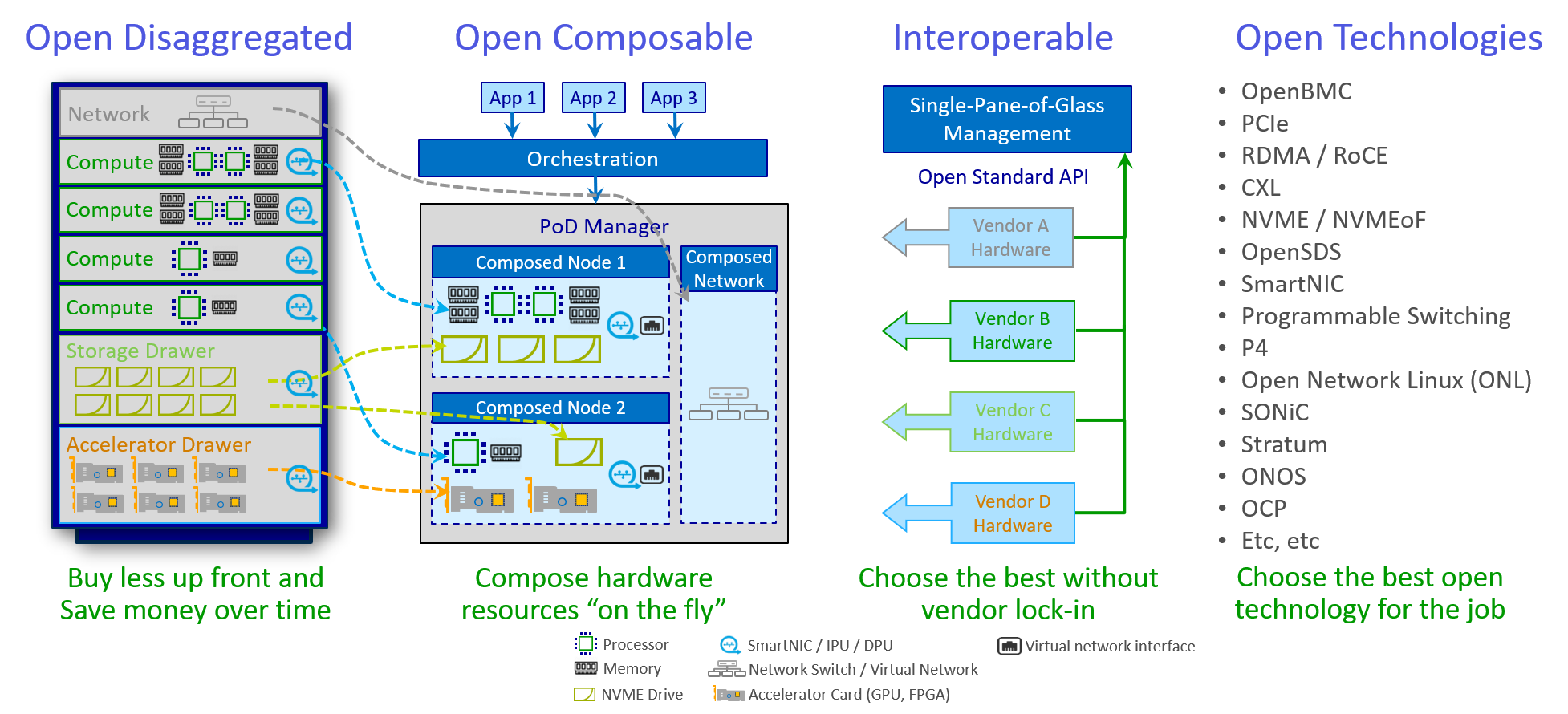
A PoD consists of hardware modules interconnected by the PoD Fabric, and controlled by control software (all in a small rack or multiple larger racks). It has a well defined standard management API and control API (for horizontal scale out) with callable generic functional products that are resource 'slices' of the PoD. Some of the network interfaces in the PoD are Network Access Points (NAP) for communication in and out of the PoD but most of them are used to interconnect hardware modules in the PoD.
In this first article I will describe the Hardware Component layer in more detail but first I will give a brief introduction of the functional products I'm targeting with this architecture. A more thorough description of functional products and the other PoD building blocks will follow in subsequent blog articles.
PoD Functional products
The combined hardware and software slices the PoD (control plane layer) can deliver, are called functional products. With those basic functional products more complex (end-to-end) services can be created by consumers of the PoD/API.
The lowest level functional products delivered by a PoD are machines. There are three hardware based machine types: Network Machine, Compute Machine and Storage Machine. Those three machine types are created from hardware components flexibly interconnected over one or more PoD wide (optical) Rack Fabric networks.
With (and on) those machines, specific services can be delivered, and those can be divided in three main groups as can be seen in figure 3:
- Network Functional Products
- Compute Functional Products
- Storage Functional Products
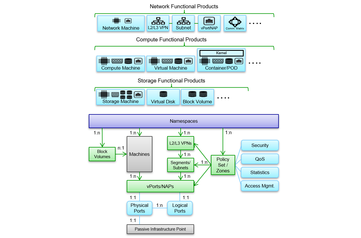
Below follows a high level description of most of the items introduced in figure 3. Hopefully this outline is enough for understanding the importance of those items for the high level vision and how they are used by the PoD control plane:
- Namespace: A representation of a set of machines, network, compute and storage services under the same administrative control. They are a way to organize a PoD into virtual sub-PoDs — they can be helpful when different service teams or projects share a physical infrastructure PoD. Any number of namespaces are supported within a PoD, each logically separated from others but with the ability to communicate with each other and share created services on network level. At startup there only exists a root namespace used for basic PoD components and PoD Control.
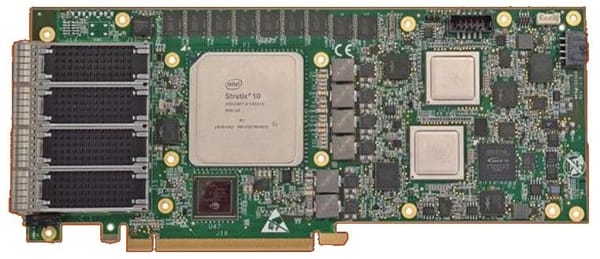
- Machines: A physical or virtual machine, or container with certain compute, memory, storage and network access point (vPort/NAP) resources attached. On this machine/container network functions or applications like for example L4+ Firewall or Load balancer can be run. An example of a specific machine is a P4 Programmable Switch with P4Runtime/gNMI/gNOI API that could be based on specific switch hardware or on a hardware accelerated plug-in card + CPU and memory.
- Block Volumes: A block volume behaves like a raw, unformatted, external block device that you can attach to a single machine. The volume persists independently from the running life of a machine. After a block volume is attached to a machine, you can use it like any other physical hard drive. Multiple volumes can be attached to a machine. You can also detach a block volume from one machine and attach it to another machine. You can dynamically change the configuration of a volume attached to a machine.
- VPN (L2/L3): One or more Segments (L2) and Subnets (L3). Can contain a logical distributed router that enables L3 communication between connected Subnets (and as such NAPs/vPorts)
- Segment: A distributed layer 2 segment that allows Ethernet communication between two or more connected network endpoints (vPorts/NAPs).
- Subnet: A distributed layer 2 segment that allows IP communication between connected network endpoints (vPorts/NAPs). A subnet can be connected to other subnets on IP level and will then be interconnected by a distributed router (to create a VPN) that enables L3 communication between connected subnets.
- vPort/NAP: A (virtual) network access endpoint that will be defined in a segment or subnet. It will be virtually interconnected with a (logical) network access point defined in a machine (NIC) or on a Infrastructure network termination unit (patch panel / physical port)
- Physical/Logical Ports: Ports that are connected outward of the PoD through a Infrastructure network termination unit (patch panel / physical port). Physical/Logical ports are administratively connected to a vPort/NAP in the Root namespace and the vPort/NAPs are then assigned to a child namespace for use in machines, segments or subnets.
- Policy Sets/Zones (Communication Matrix): Set of generic Security, QoS, Statistics and Access Control rules allowing a certain Communication Matrix between vPort/NAP/Machines etc.
PoD Hardware components
The lowest layer of a PoD consists of over the years slowly evolving basic hardware like buildings, power and cooling (all three really slow developing compared to other hardware developments). Those low level hardware building blocks are also the most expensive CAPEX (investment) wise and should have the longest technical (and financial) depreciation time to run a financial viable operation. Flexibility in housing and interconnecting the smaller modules is therefore of the utmost importance and as such a rack is a key long term building block as it brings those three (space, power, cooling) together.
Racks
The Open Compute Project (OCP) OpenRack or OpenEdge hardware designs are great examples to start with. Needed are standard pluggable racks with power busbar, management busbar and (optionally) water cooling pluggable pipes and/or pluggable fiber busbar.
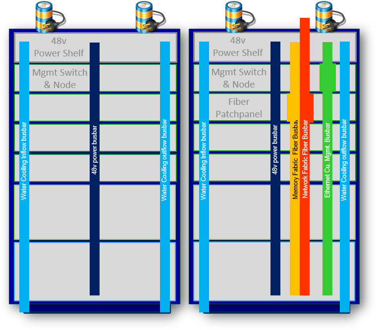
To divide the rack in smaller spaces, variable sized, pluggable drawers in the standard rack are designed with plugs to the power busbar, management busbar and (optionally) to the water cooling pipes and/or Fabric fiber busbar. In those drawers there is room for the real hardware bearing modules like for example network switch, processor, accelerator, memory or storage modules. Those pluggable hardware modules are interconnected to a Memory fabric based on PCIe/CXL and in-rack optical connections in-between drawers.
As can be seen there is at this moment a separation between the 'Memory fabric' and 'Network fabric' in communication between modules/drawers, as flexibility, latency and throughput requirements influence the technical implementation of both fabrics and the role of the IPU/DPU (Infrastructure Processing Unit/Datacenter Processing Unit) in that (see the PoD Fabric article for more background information).
The techniques driving the described disaggregation by using high speed (interconnected) memory fabrics are still in full development at this moment. Major technologies used here are the next generations of PCIe (5, 6, 7, ...), Compute eXpress Link (CXL), Silicon Photonics and in-package optical IO. See the next paragraphs for more background information.
PCIe and Compute eXpress Link (CXL)
First of all PCIe (Peripheral Component Interconnect express). PCIe is at the moment the interface and communication bus standard for connecting high-speed hardware components in one box. And anybody doing something in the ICT industry should already know the basics about it ;-).
Most people know PCIe from its physical and data link layer definitions like speeds, lanes and x1, x2, x4, x8 and x16 specs. But maybe most important is the transaction layer standard that makes it possible to communicate between devices and implement a multi device switched fabric between devices.
Unlike its PCI predecessor, which used a shared parallel link bus as physical and data link layer, PCI Express is a switched architecture of up to 32 independent, serial lanes (x1-x32, but you'll currently never see x32 in real implementations!) that transfer in parallel. Each lane is full duplex.
PCIe standards currently come in five different generations: PCIe 1.0, through PCIe 5.0. Up until now the bandwidth of the main components of the bus (serial bi-directional lanes) double with each generation and also the PCIe switching standard is extending the number of components that can be interconnected.
The newest official standard (PCIe 5.0) came out in May 2019. It will bring about 504 Gbits/s of throughput with 16 lanes (about 32 Gbit per lane). The specification is backwards compatible with previous PCIe generations and also includes new features, including electrical changes to improve signal integrity and backward-compatible CEM connectors (the connector strips) for the well-known add-in cards. The first PCIe 5.0 devices are expected to debut for enterprise customers in 2021.
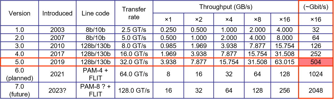
The next release of the standard (PCIe 6.0) is scheduled for end of 2021. Currently the specification document is at version 0.7 which means that the release is closed for new functionalities and that all low level technical tests are concluded positively. So it is waiting now on the final 1.0 version. Within the 6.0 release the biggest changes is the use of PAM-4 line encoding and the use of 256 byte large FLIT encoding with included synchronisation, lightweight CRC and retransmission instead of separate synchronisation bytes, heavy CRC and variable length message sending. (old telecom guys: like ATM's fixed size cell 🙃).
This all needs to be done to keep/get the the link latency below 10 ns and let PCIe to be the physical and data link layer for not only PCIe but also for other component interconnect protocols like CXL (see below), CCIX (Cache Coherent Interconnect for Accelerator), UPI (Intel Ultra-Path Interconnect), IBM XBus protocol, Nvidia NVLink protocol, AMD Infinity Fabric protocol, cache coherent interconnect for accelerators (CCIX) protocol, coherent accelerator processor interface (OpenCAPI) and other inter-chip protocols. This all looks disrupting but the PCI-SIG is saying it will all be backwards compatible with older PCIe releases.
As already mentioned, another important new development (version 1.0 released in 2019) on top of PCIe is Compute Express Link (CXL). CXL is a mix of (FLIT message!) protocols meant to help processors of compute systems, especially those systems with accelerators, operate more efficiently. CXL currently sits atop the PCIe 5.0 data link infrastructure (and also copies parts from the transaction layer) but is also backwards compatible with lower PCIe versions (to version 3.0 in CXL degraded mode) and is more or less the PCIe Transaction Layer on steroids. Many PCIe 5.0 devices will also support the ability to run their lanes in either PCIe or CXL transaction modes.
Instead of being a vendor-specific implementation, this is a broad industry standard. The key advantage of CXL is it allows load/stores to happen to memory that is directly attached to different endpoints. Memory is a key driver for this as almost every device these days has onboard memory, and memory both is a large cost driver and also is often stranded by being under-utilized by the device it is attached to. At a higher level, CXL is a tool for systems to efficiently (coherently) share and utilize memory across a number of devices.
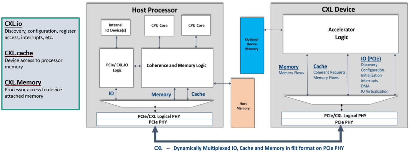
CXL uses three main protocols (figure 8):
- CXL.io is the protocol used for initialization, link-up, device discovery and enumeration, and register access. It provides a non-coherent load/store interface for I/O devices and its definition and implementation is similar to the PCIe defined function. It also is mandatory that all CXL devices support CXL.io.
- CXL.cache is the protocol that defines interactions between a Host (usually a CPU) and Device (such as a CXL memory module or accelerator). This allows attached CXL Devices to cache Host memory with low latency, like a GPU core directly caching data stored in the CPU’s memory.
- CXL.memory is the protocol that provides a Host processor (usually a CPU) with direct access to Device-attached memory using load/ store commands. Examples: the CPU using a dedicated storage-class memory Device or using the memory found on a GPU/accelerator Device.
CXL.io is mandatory to get an endpoint on CXL, plus any of the three combinations of CXL.cache and/or CXL.memory.
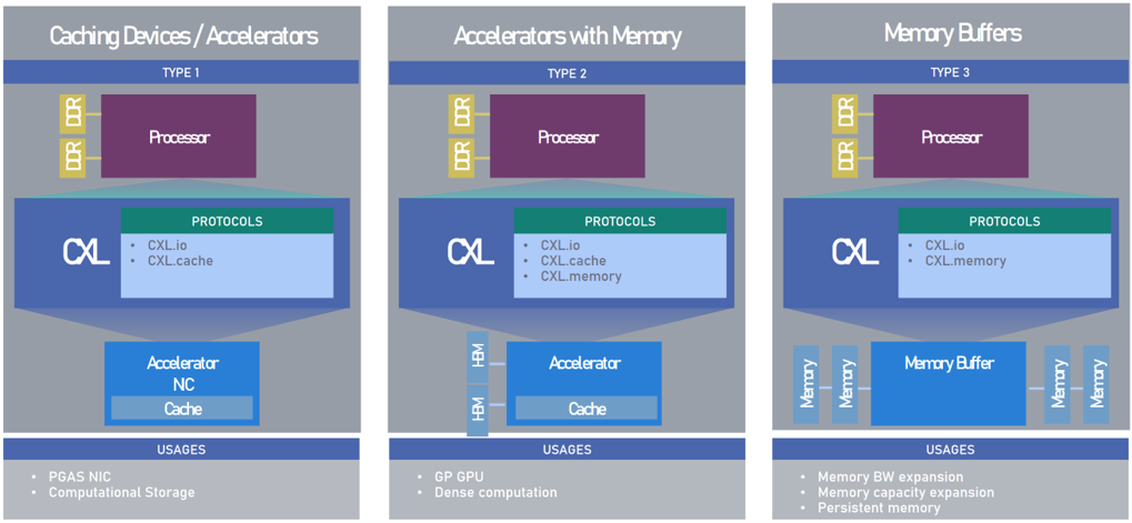
There are three standard device types defined:
Type 1 (CXL.io + CXL.cache) - an accelerator like a NIC that accesses the host CPU’s memory directly.
Type 2 (all three protocols) - an accelerator, like a GPU with memory, can access host memory while the host CPU can access GPU memory.
Type 3 (CXL.io + CXL.memory) - primary purpose is to expose the CXL memory device media to the host CPU.
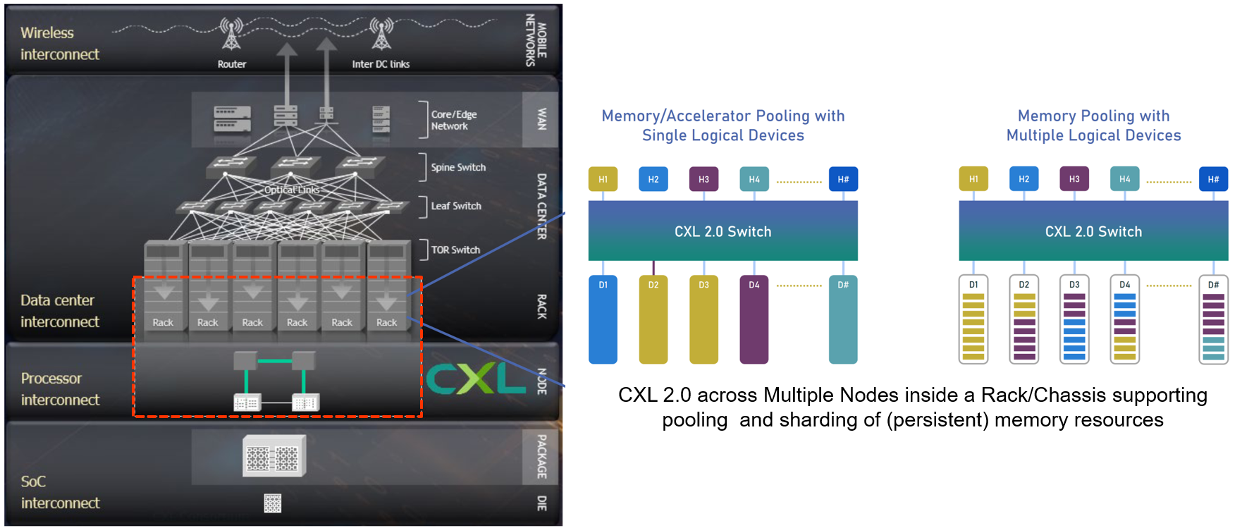
The latest version of CXL (2.0, nov 2020) made it also possible to use CXL switches, persistent memory devices and device pooling for even more flexibility in location and shared use of hardware modules.
The existing and upcoming future generations of PCIe and CXL will make it possible to flexibly create highly integrated, high performance compute, storage and networking machines out of every combination of devices plugged in racks with generic drawers and optical connections (see next paragraph).
Silicon Photonics and In-package optical I/O
Another important area of innovation is in-package optical I/O. In-package optical I/O technology is the first solution to enable direct optical communications instead of copper electric communications between key components in data center systems, including GPUs, CPUs, APUs, HBM and pooled memory. This is driven by new Silicon Photonics technologies that enable miniaturizing and mass scale production of optical components.
The electro-optical approach eliminates bandwidth issues by driving a 100 – 1,000x improvement in interconnect bandwidth density as well as better latency and lower power requirements. With respect to latency, raw in-package optical messaging supports end-to-end off package connections of ~10 ns plus time of flight (5 ns/m) versus ~100 ns plus time of flight (5 ns/m) for Ethernet. From a power perspective, the technology requires roughly a 10th of the power needed to move a bit of data electrically. It also underpins more flexible systems by enabling innovative dis-aggregated and distributed architectures.
Ultimately, a key advantage of optical interconnects is that they eliminate key impediments to scaling, including the need for system and application software designers to factor in explicit latencies and communication patterns between compute resources.
Figure 11 below is a conceptual graphic of in-package optical I/O providing increased bandwidth with shared pooled memory. This dis-aggregated solution enables direct, lower-latency access to DRAM for a collective of GPUs, as well as CPU and GPU/APU access to common, shared large-capacity memory. In-package optical I/O allows seamless chassis and rack-scale scale-out between XPU-MCPs and pooled DRAM memory modules over CXL fabric as an example, with in package enabled CXL switches expanding the scale-out to system-scale.
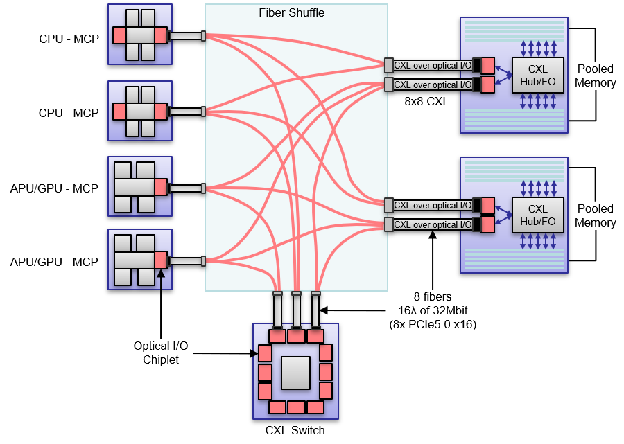
In-package optical IO and future photonic switches promise to have a large impact on future high performance compute and data center networks. However, even with CXL, optical IO and photonic switches alone, we cannot achieve significant system-wide benefits if we do not change the rest of the system architecture. This motivates co-design between emerging technologies and the rest of the system in order to adapt the system network to best make use of unique features of new optical technologies, as well as tailor those to better support system-wide trends such as resource dis-aggregation.
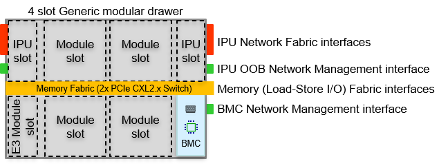
Drawer Modules
One example of changing the system architecture by using PCIe 5.0, CXL and in-package optical technologies is in the rack 'drawer' space. Multiple drawers and modules inserted in a rack could be high speed (optically) interconnected and can represent one large pool of hardware resources to be used to create flexible sized "machines".
Examples of standard modules that could be inserted in drawers and used to create 'machines' with, are:
- Compute (xPU) modules (boards) with local high speed memory and a PCIe/CXL interface. For example x86, ARM, GPU, ASIC processors and memory on a PCIe pluggable module.
- Storage/Memory modules with local controller and high speed (persistent) memory with pluggable fast storage (for example Solid State Memory as NVMe SSD's) and a PCIe/CXL interface.
- Networking modules with network switch ASIC + different number and speed of interfaces, and a PCIe/CXL interface to the bus for connection to a compute module implementing the local network control layer or an API to a distributed control layer.
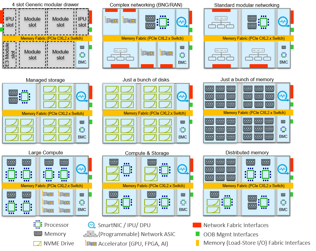
The next two paragraphs describe some OCP and EDSFF design formats which implement and define different standard modules that could be used in these example standard drawer designs.
OCP based Compute and Accelerator module formats
Artificial Intelligence (AI) applications are rapidly evolving and producing an explosion of new types of hardware accelerators for Machine Learning (ML), Deep Learning (DL), High-performance Computing (HPC) and High-performance Networking (HPN).
Different implementations target similar requirements for power/cooling, robustness, serviceability, configuration, programming, management, debug, inter-module communication to scale-up, and input/output bandwidth to scale-out.
To take advantage of the available industry-standard form factors to reduce the required time and effort in producing suitable solutions, various implementations have selected PCIe CEM form factor (the standard PCI card) as a quick market entry. Such solutions are not optimized for the upcoming AI workloads which require ever-growing bandwidth and interconnect flexibility for data/model parallelism. The state-of-the-art applications require multiple cards in a system with multiple inter-card links running at high speed interconnect bandwidth between cards.
The OCP Accelerator Mezzanine Module design specification was the first to define a form factor and common specification for a compute accelerator module and a compliant base board (rack drawer module) design, enabling interoperability across multiple ASIC or GPU based mezzanine modules and a based board design interface.
The mezzanine module form factor facilitates scalability across accelerators by simplifying the system solution when interconnecting communication links among modules in comparison with a PCIe Add-in card form factor.
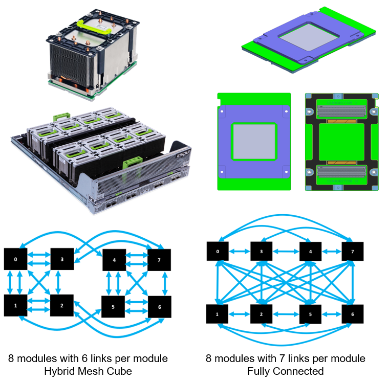
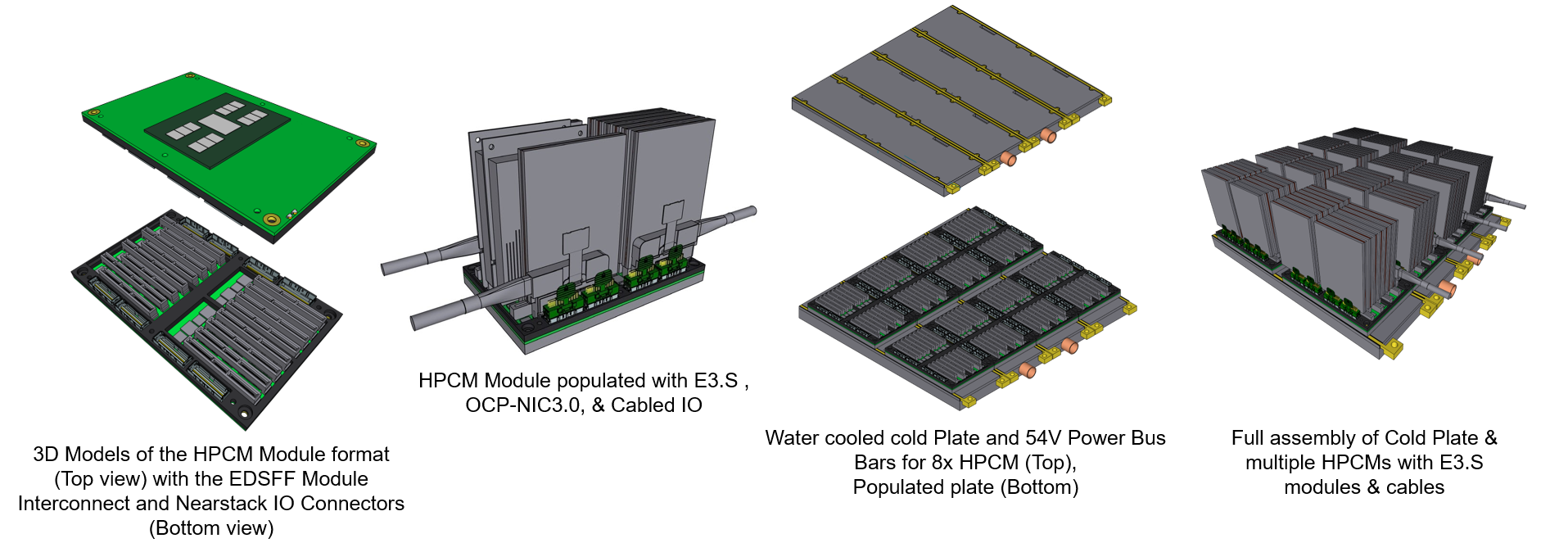
Next to the OAM design also work on a high performance compute module (HPCM) design has started. The current work in progress of the primary modular architecture for HPCM is inspired by the OAM format and as such the overall size of 165mm x 102mm has also been used for the HPCM format. See figure 14 showing 3D Models of the format with the water cooled multi module base cold plate, EDSFF Module Interconnect and Nearstack IO Connectors.
If this HPCM format gets through the specification phases and has use with the hyper scalers, this will also be a serious new development for the modular vision for operators and enterprise infrastructures.
EDSFF based standard module form factors
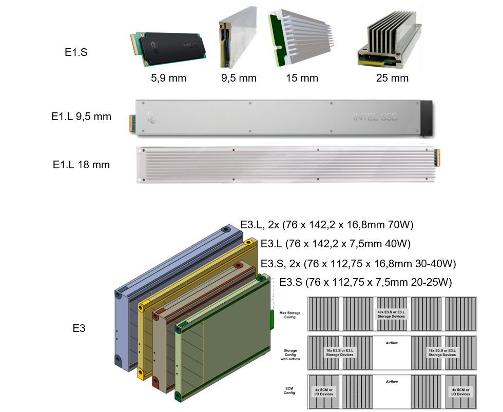
Another organization working on standardizing storage modules is the Enterprise & Data Center SSD Form Factor working group (EDSFF). Starting from a storage perspective the EDSFF designed several form factors for use as NVME based storage modules. During the design phase of the E3 form factor several vendors saw the opportunity to extend it for use for pluggable compute accelerators, FPGAs, OCPv3 NIC and CXL based memory modules. Currently 2 major formats are important, E1 and E3.
E1 - Flexible Form Factor (1U high):
- Family of devices allows multiple device types with different power profiles
- Common device bay mechanics (smaller devices fit into larger device bays)
- For scalable & flexible performance storage
E3 - Flexible Form Factor (2U high):
- Family of devices allows multiple device types with different power profiles:
- E3.S - Optimized for primary NAND (solid state) storage in servers.
- E3.S 2x - Support for higher power devices like CXL based SCM (Storage Class Memory)
- E3.L - Support for higher capacity NAND storage.
- E3.L 2x - Support for higher power devices like FPGAs, accelerators and OCPv3 NIC. - Common device bay mechanics (smaller devices fit into larger device bays)
- Supports multiple link widths (x2, x4, x8, and x16)
- Requires a mechanical device carrier which allows for OEM ID customization
Examples of current modular hardware implementations
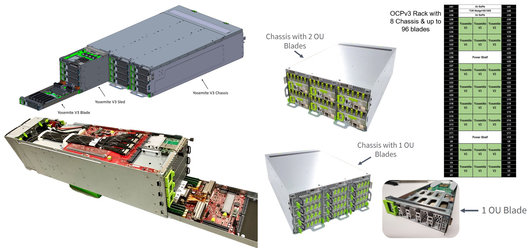
The previous described technologies are still mostly in development or not widely available and the really multiple optical drawer/rack disaggregated hardware implementations are not there (yet)! But there are already current implementations of near flexible open way of hardware stacks, like for example some designs created by members of the Open Compute Project (OCP). One of them is the Yosemite V3 implementation which is available to the 'normal public' too and also allows EDSFF module use.
Although it doesn't have a PCIe bus extension between different Yosemite V3 chassis it could be implemented in the future by a (still to be created) shared OCP (IPU) PCIe/NIC card for example.
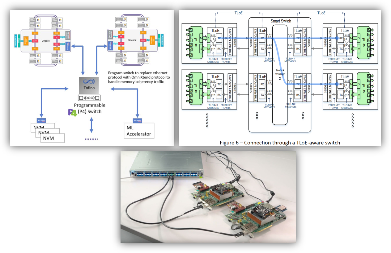
Another example of a real live experiment and implementation of CPU and Memory disaggregation is for example RISC-V OmniXtend. Imagine in-package optical IO in this design and think of the possibilities. See the next figure and this link for more information.
Summary
First the generic idea and vision was described, the term Infrastructure PoD and the important Infrastructure PoD building blocks where introduced. After that I went in some more detail on two of the main Infrastructure PoD building blocks: Functional Products and Hardware. We learned that to get real disaggregation advantaged and composability the PoD Fabric layer is very important.
The next article in this series will touch PoD Fabrics. After this initial series I intend to have follow-up articles explaining Network, Compute & Storage composition and implementation + other articles explaining emerging new technologies in more detail.
If you have any questions or other remarks you can contact me through email (see the contact tab on the top of this page) or on twitter (@stolsma).